Transmission Electron Microscopy
Fall 2021
As part of my Electron Microscopy Fundamentals course in Fall 2021, I had the chance to work with an FEI Tecnai F-20 transmission electron microscope (TEM). Some of the basics of what we learned included:
- Loading of samples by placing in holder, filling liquid N2, inserting holder into chamber, and waiting for vacuum to establish.
- Finding eucentric position using: 1) alpha wobble and minimizing image movement 2) minimizing visibility of image on fluorescent screen above camera 3) collapsing diffraction rings into a single spot.
- Operating the tool with both the software and the control board.
Below I discuss specific topics we covered in lab.
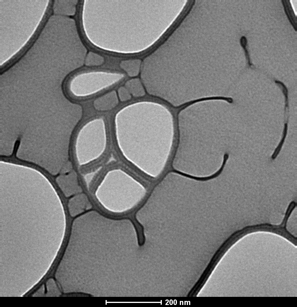
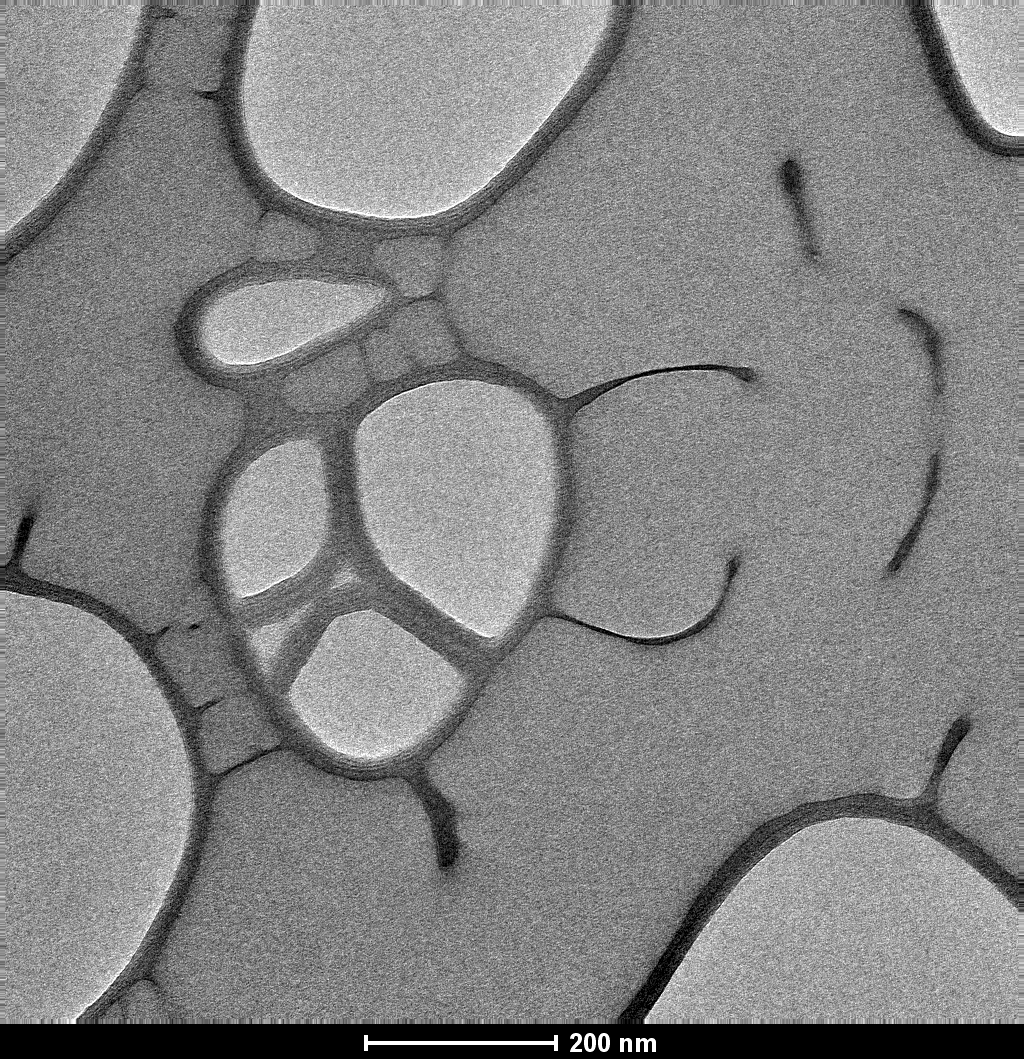
Fresnel Fringes
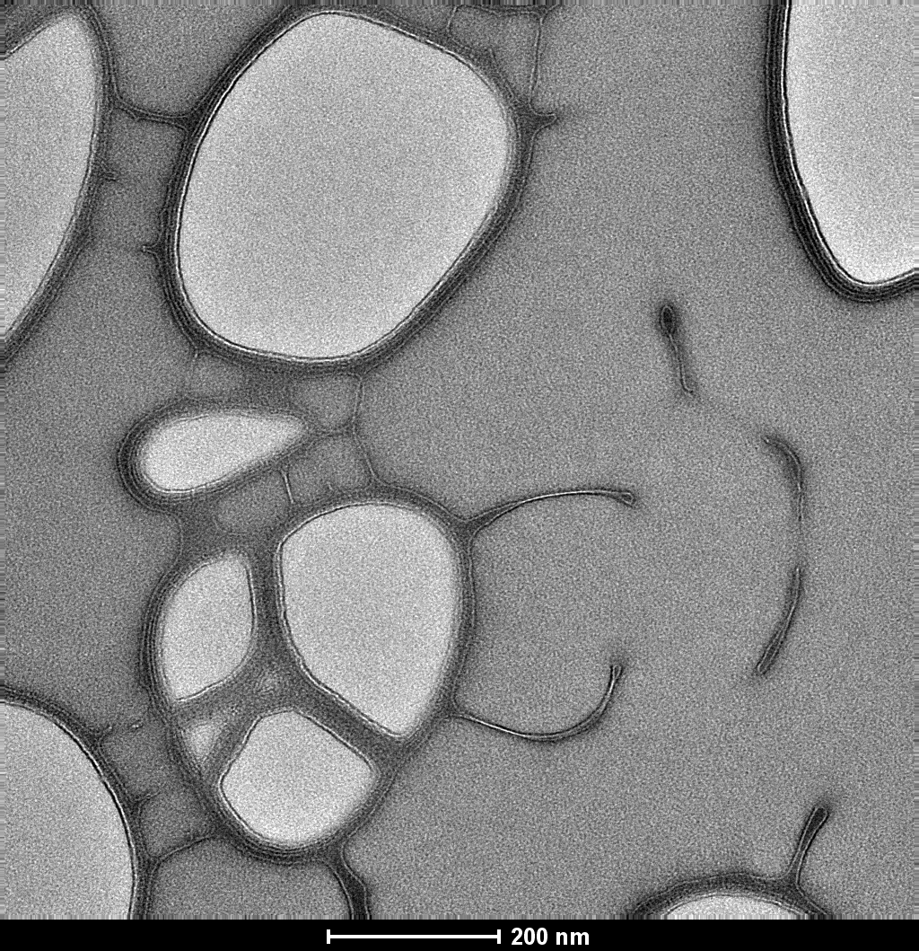
A common method of finding focus in a TEM is with so-called Fresnel fringes. Shown below are images of a lacy carbon sample at different levels of focus. The bright areas are holes in the carbon while the dark areas are the carbon network. At an underfocus, a bright fringe can be seen at the edge of the bright regions. On the other hand, an overfocus causes a fringe effect along the edge of the dark regions.
True focus is obtained by minimizing the appearance of these fringes, but at the cost of reducing the contrast in the image. For this reason, it's useful to take images at a slight underfocus to improve clarity of sample features.
Diffraction Patterns
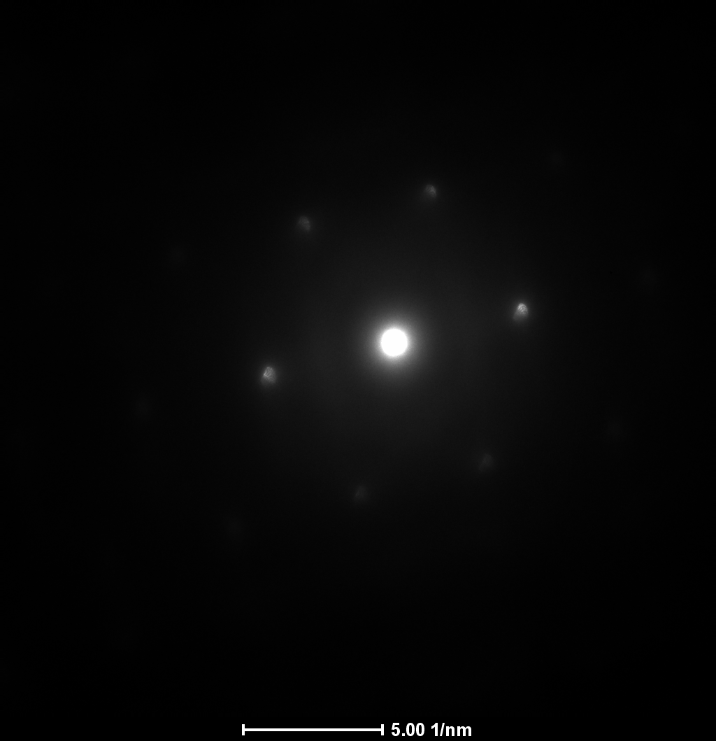
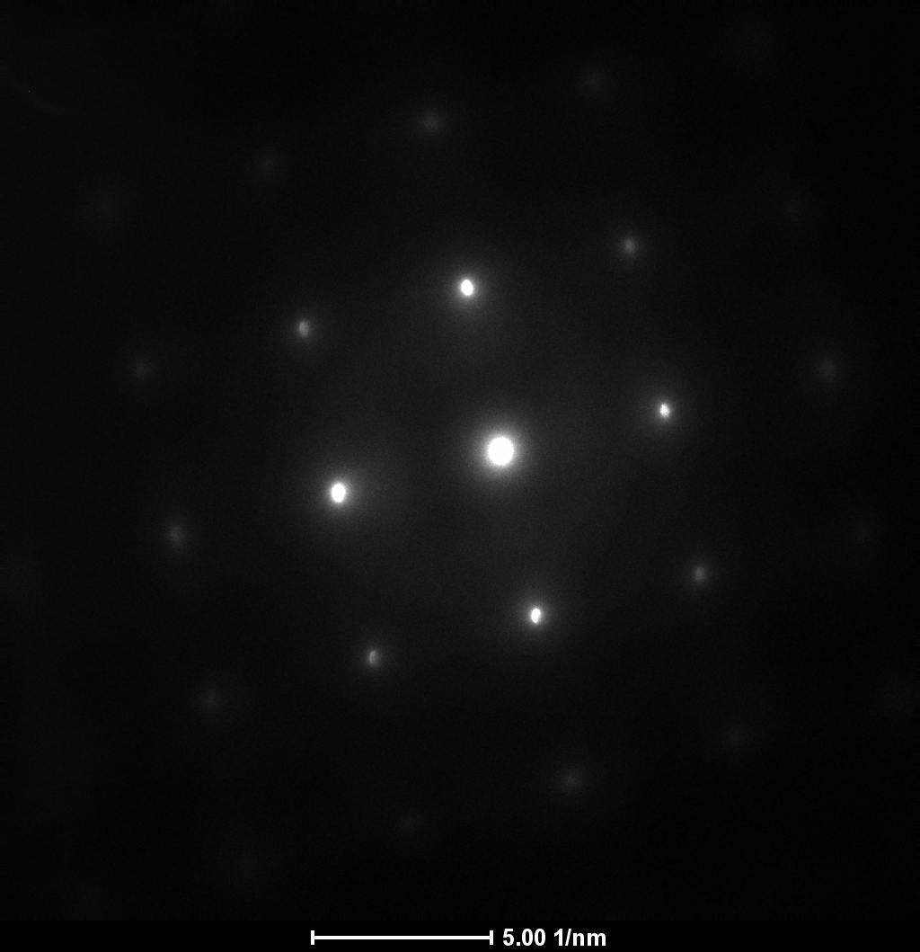
One of the strengths of a TEM is the ability to view diffraction patterns of materials. The diffraction pattern of a material can provide information on its crystal structure (or lack thereof) and it's atomic composition. It's worth noting the diffraction pattern is a Fourier transform of the image plane.
Pictured below are diffraction patterns of two different monocrystalline samples. The diffraction patterns were obtained by following the so-called "Kikuchi lines" while in diffraction pattern imaging mode. Tilting the sample in two directions (alpha and beta tilt) guided the lines towards a crystal face (zone axis) in the sample so a spot diffraction pattern could be seen.
We only briefly discussed identifying crystal structures and elements from their diffraction patterns. My guess for the right pattern is silicon. The other remains a mystery, though it appears to be a cubic structure.
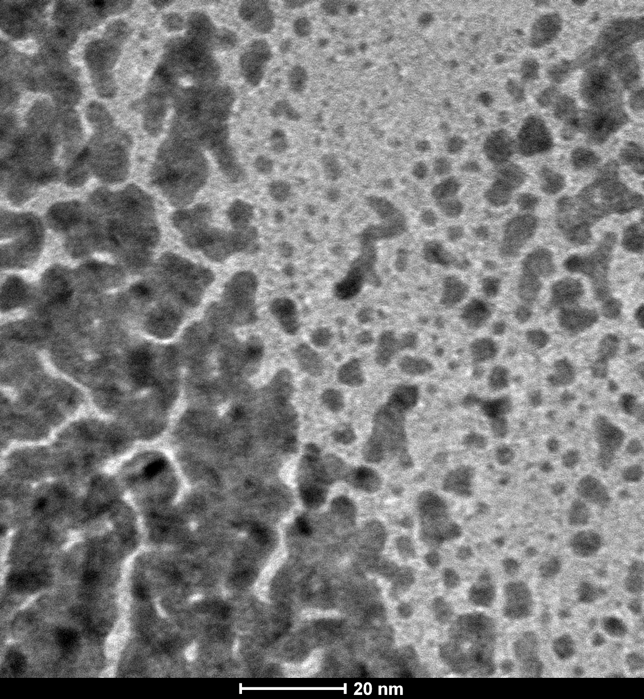
High Resolution TEM
The final lab of the course tasked us with resolving individual atoms of gold. This meant pushing the Tecnai to its resolution limits, which required shrewd application of our basic focusing techniques along with new ones.
As we stepped up the magnification, we iterated back and forth between finding focus, adjusting for beam stigmation, and setting the rotation center for the sample. An important difference from our previous imaging was the removal of the objective aperture to use phase contrast rather than amplitude contrast. Other considerations were:
- Tilting the sample to find a zone axis, so that some of the planes of atoms in the sample were perpendicular to the beam,
- Using the defocus knob to gain a bit of extra control over the focus than the Z-height control could provide.
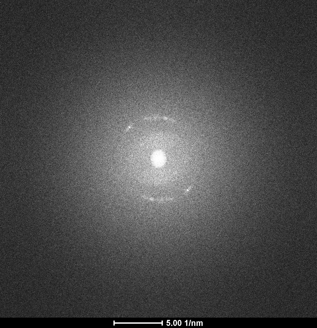
If you scan through the image below, you can find regions where the fuzziness gives way to a fabric-like texture. Those textured areas are columns of gold atoms. Another piece of evidence for their presence in the image below is the image's Fourier transform: It is just possible to see spots in it's rings, indicating the crystal structure of the material is visible.