Scanning Electron Microsocopy
Fall 2021
As part of my Fundamentals of Electron Microscopy Course, I had the chance to work on a Thermo Fisher Apreo 2 SEM. The course covered a variety of applications, including:
- secondary electron (SE) imaging,
- backscatter electron (BSE) imaging,
- low vacuum imaging (i.e. water vapor for charge conduction),
- sample preparation,
- energy-dispersive x-ray spectroscopy (EDS),
- and a niche use of an insulating material as an electron mirror!
Below I talk about each application alongside example images.
SE Imaging
Secondary electrons are displaced from the sample by the high energy electron beam. They are one of the two main types of electron emission.
Imaging with secondary electrons allows capture of fine surface detail. This is because their low energy prevents them escaping from "deep" inside the sample. SE detection can be encouraged by applying a positive to the detector.
BSE Imaging
Backscattered electrons originate from the electron beam. They return out of the sample after scattering events such as deflection or collision.
Imaging with backscatter electrons allows features or atomic identity below the surface of the material to be probed. It is possible to discriminate for BSE detection by applying a negative bias to the detector.
Sample Preparation
There are two main concerns when preparing SEM samples:
- Charge conduction is needed to image the sample.
- The key characteristics of the sample need to be preserved.
The method of sample preparation I have the most experience with is sputter coating. It addresses the charge conduction need by coating the sample in a thin layer of metal using vapor deposition. Gold and palladium are commonly used--likely to avoid undesirable oxidation while transporting the sample.
Sputter coating is not suitable for heat sensitive materials and is likely to damage organic specimens. Some damage can be seen in the curling of the stone paper I tried to sputter coat! The regular paper and fly (not mine) didn't show signs of damage.
Low Vacuum Imaging
Sample preparation methods often involve some degree of damage to a sample. Low vacuum imaging provides a way to image insulating samples without any preparation. A small amount of water vapor is added to the chamber with the sample. This water vapor is ionized by the electron beam and acts as the vehicle for dissipating charge.
The introduction of water vapor in the chamber reduces the maximum imaging resolution, so there is a price to pay (beyond the dollar cost). This is shown in the pair of images on the left. The first is an image of sputter coated stone paper imaged in SE mode at 25000x, while the second is an image of uncoated stone paper at 10000x using low vacuum imaging. Compared to optical microscopy, the low vacuum results are impressive, but there is a significant loss in maximum resolution from standard SEM imaging.
EDS
Energy-dispersive x-ray spectroscopy is a natural addition to an SEM's toolkit. The electron beam excites the electrons of the sample into higher states, leading to the generation of characteristic spectra. The spectra can be used to identify relative amounts of elements.
Some advantages of EDS are that it can be quick and isn't any more destructive than the electron beam itself. However, it is mostly limited to relative quantitative analysis. Absolute quantitative analysis is difficult, though it can be done by by collecting spectra from a reference sample of known composition.
Shown to the right are spectra for premium bright printer paper stone paper. The printer paper spectra is quite simple--we see gold and palladium peaks from the sputter coating and carbon and oxygen peaks from the organic material of the paper. Things are more complicated in the stone paper spectra. The software identified several small peaks. These don't give much insight beyond indicating trace amounts of magnesium seem to be present. We also see clear readings of carbon, oxygen, and calcium. All this makes sense as stone paper is made out of limestone--i.e. calcium carbonate (CaCO3).
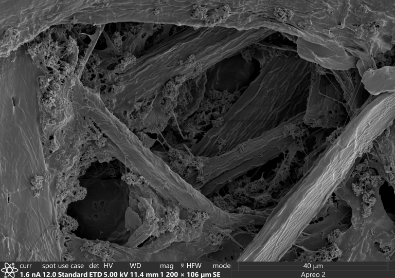
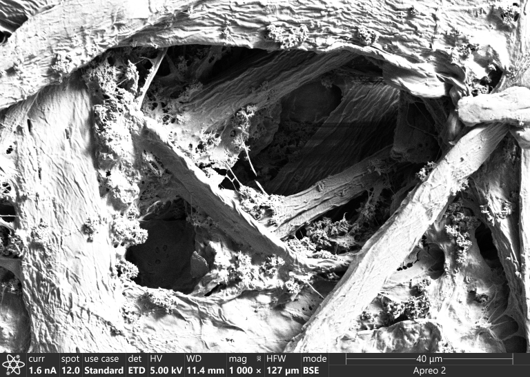
Electron Mirror
It's generally important for samples to be conductive. Insulators hold on to charge from the beam and prevent imaging of the sample. However, this property can be exploited to create an electron mirror.
Below are images of the chamber of an Apreo 2 SEM. The images were collected by directing the beam at a piece of plastic. The first image was collected using secondary electrons (SE) and has good clarity apart from the charging streaks towards the top right. Imaging again with back-scatter electrons (BSE) removed most of the charging effect but reduced clarity. In a third attempt, the mirror was imaged again in SE mode at a lower magnification. This removed the charging effects while keeping the original clarity, albeit at the cost of less detail (contrast was also adjusted to reduce saturation around the nosepiece).